Canceled overview - All Canceled
Primary tabs

The HW Group continuously innovate products to provide state-of-the-art technology, security, and software tools. Many accessories and innovations are available for older units in operation. An overview of older product versions makes it easy to select and offers overview of device backward compatibility.
Device
-

STE2
WiFi and Ethernet, PoE available, temperature and humidity sensor with digital inputs.
Product canceled New product Available
-

SD-WLD
1x Water Leak Detection zone (sensing cable) to the portal. LAN and WiFi connectivity, IoT Monitoring unit (Portal required).
Product canceled
-

SD-2xOut
2x DO (Relay Output) controlled from the portal. LAN and WiFi connectivity, IoT Monitoring unit (Portal required).
Product canceled
-

SD-2xIn
2x DI (Digital Input) for external door / smoke detectors, S0 counters. LAN and WiFi connectivity, IoT Monitoring unit (Portal required).
Product canceled
-
")
SD-2x1Wire
4 external RJ11 sensors values to the portal (Temperature, Humidity, Voltage, and many others). LAN and WiFi connectivity, IoT Monitoring unit (Portal required).
Product canceled
-

SD 4-20mA
1x AI (Analog Input) for external 4-20mA / 0-20mA probes. LAN and WiFi connectivity, IoT Monitoring unit (Portal required).
Product canceled
-

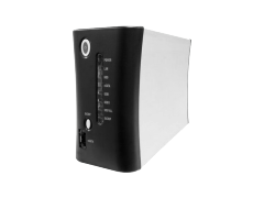
Poseidon2 3266
Cost-effective model for remote monitoring of sensors and detectors.
Product canceled
-

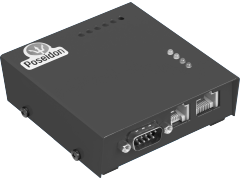
Poseidon 4002
Poseidon 4002 is a 19" 1U rack mount system for datacenter temperature and environment monitoring. The Poseidon solution monitors racks and computer rooms (temperature, humidity, electricity supply, access to the room, detectors).
Product canceled New product Available
-
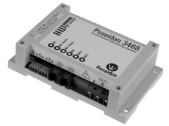
Poseidon 3468
Web enabled thermostat with temperature/humidity measurement, four dry contact inputs and two 110/230V relay outputs. Industrial version, supports SNMP and E-mail, DIN rail mount.
Product canceled New product Available
-
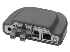
Poseidon 3268
Ethernet temperature / humidity monitoring with 2 relay outputs and 4 dry contact inputs (Web, SNMP, and E-mail). Output relays can be controlled over the Web.
Product canceled New product Available
-
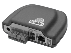
Poseidon 3266
Temperature / humidity measurement and monitoring of 4 dry contacts over a LAN (Web, SNMP, E-mail). A MS Excel reporting software with is graphs included for free.
Product canceled New product Available
-
Poseidon 2250
Poseidon 2250 logs the values from up to 40 probes (RS-485, dry contacts, temperature, voltage, and more).
Product canceled New product Available
-
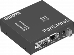
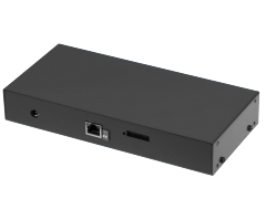
PortStore5
RS-232 and RS485 full serial port to Ethernet converter with a buffer.
Product canceled
-

IP WatchDog Lite
IP WatchDog Lite monitors function of Ethernet devices.
Product canceled
-

IP WatchDog HWg-WR02a
Monitors the functionality of a device over IP (PING/WEB) or serial line (RS-232), automatically restarts it upon failure.
Product canceled New product Available
-

IP Relay HWg-ER02a
The IP Relay ER02a is a RS-232 / RS-485 serial line converter with two 230V-rated SPDT relays.
Product canceled New product Available
-

HWg-WLD
Water leak detector with Ethernet connectivity that detects water in a "2D area" using a sensing cable.
Product canceled New product Available
-

HWg-STE plus
Ethernet temperature and humidity sensor with digital inputs.
Product canceled New product Available
-

HWg-STE
Ethernet temperature and humidity sensor.
Product canceled New product Available
-

HWg-SiteMon5
Remote monitoring of telecom sites and equipment rooms over LAN. Supports sensors for voltage, current, temperature, door, water leak, energy
Product canceled
-
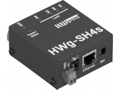
HWg-SH4s
The HWg-SH4s a door unlocker subordinated to the HWg-SH4 unit. HWg-SH4s unit opens one electromagnetic lock.
Product canceled
-
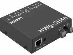
HWg-SH4e
The HWg-SH4e a door unlocker subordinated to the HWg-SH4 unit. HWg-SH4e unit opens two electromagnetic locks.
Product canceled
-

HWg-SH4
An access system for opening any kind of electromagnetic lock with any RFID reader.
Product canceled
-

HWg-SH3: IP-based Rack Access Control System with RFID
HWg-SH3 is a cabinet IP Access Control System (ACS) with RFID interface. User database is configurable over the Web.
Product canceled
-

HWg-SH2: IP-based cabinet access system for two swinghandles
Online cabinet Security Door Control (SDC) with Web & SNMP interface. HWg-SH2 can control front & rear doors of one cabinet. Swinghandle lock access system is controller over IP using documented M2M protocols.
Product canceled
-
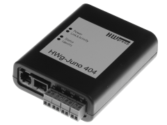
HWg-Juno 404
HWg-Juno 404
Product canceled
-

HWg-Juno 1200
HWg-Juno 1200
Product canceled
-

HWg-Juno 101
Product canceled
-

HWg-Juno 008
HWg-Juno 008
Product canceled
-
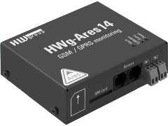
HWg-Ares14
HWg-Ares14 is a remote environment monitoring solution that can be used at any place with GSM coverage. Contains a battery for several hours of backup.
Product canceled New product Available
-

HWg-Ares 10
Cost-effective GSM thermometer with remote management and alerts sent by e-mail, text messages or by dialing a number.
Product canceled
-

Damocles MINI
Damocles MINI is Web-relay with 4 digital inputs and control 2 NO/NC relay outputs over the Web and M2M (SNMP, XML, Modbus/TCP).
Product canceled New product Available
-

Damocles 2404i
Damocles 2404i features 24 dry contact inputs and 4 relays controlled over an IP network (Ethernet). Includes a built-in web server, output control and alarm alerts (e-mail and SNMP trap).
Product canceled New product Available
-

Damocles 1208
Damocles 1208 is a device with 12 remote inputs and 8 outputs over Ethernet with Web interface. M2M communication for connection to SNMP and SCADA systems.
Product canceled New product Available
-

Ares 10 LTE
Economical GSM and LTE thermometer with remote management and alarm via ringing, SMS and e-mail.
Product canceled
Sensor
-

Temp-485-Pt100 version "Frost"
Temperature probe for extremely low temperature measurements, equivalent to "Cable" version
Product canceled
-

Temp-485-Pt100 "Head"
Temp-485-Pt100 "Head"
Product canceled
-

Temp-485-Pt100 "DIN"
Temp-485-Pt100 "DIN"
Product canceled
-

Temp-485-Pt100 "Cable2"
An IP65 protected box for wall mounting, containing RS-485 converter (Temp-485-Pt100 „Head“ version). Pt100 sensor not included.
Product canceled New product Available
-

Temp-485-Pt100 "Cable"
Temp-485-Pt100 "Cable"
Product canceled
-

Temp-485-Pt100 "Box"
Temp-485-Pt100 "Box"
Product canceled
-

Temp-485-2xPt100 DIN
Temp-485-2xPt100 "DIN"
Product canceled
-

Temp-1Wire (1m, 3m, 10m)
Temperature probe (-10°C to +80°C) designated for IT environment, for installation into IT cabinets (racks) to a cable bundle.
Product canceled New product Available
-

Temp 1Wire Pt1000 Frost
Precise industrial temperature sensor -200 to +160 °C
Product canceled New product Available
-

Temp 1Wire Pt1000
High precision temperature sensor -50 °C to 200 °C - ideal temperature sensor for storages, food processing, freezers, medical and laboratory environments, agriculture and industrial applications.
Product canceled New product Available
-

Sensor 60V 1W-UNI
Electrically isolated voltage sensor for up to 60VDC with 1Wire-UNI output. Typical applications include measuring voltage at industrial sensors (0-10V) or battery voltage.
Product canceled New product Available
-

Sens-485-UI
Product canceled
-

Sens-1W-UDI86
Product canceled
-

Pt30 - 2m Pt100 version
Product canceled
-

PowerEgg
Product canceled New product Available
-

HTemp-1-Wire Outdoor old
Temperature (-30°C to +85°C) and humidity sensor for outdoor use, communicating over 1-Wire bus (MicroLan). The sensor is designed for connecting to Poseidon, Ares and STE units.
Product canceled New product Available
-
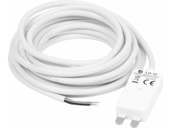
Flood detector LD-12
A simple contact water leak detector.
Product canceled
-

Door contact
Detects door opening / closing. It is typically used to extend the functions of access systems or as a detector connected to Damocles or Poseidon2 units.
Product canceled New product Available
-
DHZ 5/63-M-Bus
Single-phase electrocity meter 63A with M-Bus
Product canceled New product Available
-

30A Current probe 1W-UNI
30A Current probe 1W-UNI is a 1-Wire sensor for indirect (without cutting the wire), single-phase measurement of AC current up to 30A.
Product canceled New product Available
Accessory
-

WAGO I/O block tool
Hand tool for Terminal IO strip "WAGO" handle. Small Screwdriver can be used as well.
Product canceled
-

RFID tag
This RFID tag is EM4102 chip with unique code of 64bits.
Product canceled
-

RFID Reader R3 - RJ45
RFID reader in standard EM4100 (125kHz) with keyboard and interface of Wiegand.
Product canceled
-

RFID reader R3
RFID reader in standard EM4100 (125kHz) with keyboard and interface of Wiegand.
Product canceled
-

RFID card M1
RFID Card type M1. White card with HWg logo & printed order code.
Product canceled
-
. Suitable for Poseidon2 and Damocles2.")
PowerStripDC
DC Power Strip splits 12VDC power from a power adapter to connect other devices (e.g. a flood or smoke detector).
Product canceled
-
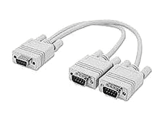
Poseidon x2 serial splitter
Serial port splitter cable for connecting Poseidon RC Cable (2 relay outputs) to GSM modem.
Product canceled
-

Poseidon B-Cable
RS-485 bus is used for connecting sensors to a Poseidon unit for up to 1 000 meter distance. RS-485 sensors uses 4 wires connection (A, B, +, -) or standard RJ45 connectors. B-Cable module converts these two ways of connection.
Product canceled
-

Poseidon 1250 Relay cable
Converter for connecting of two relays to 12V to Poseidon 2250 over RS-232
Product canceled
-

Modem Cable Poseidon 1250/2251
Cable for connecting a GSM modem to Poseidon 2250. (Only RxD, TxD a GND signals are connected).
Product canceled
-

LTE router LR77 v2 Libratum
Balanced router LR77v2 Libratum a LTE, non-modular wireless router features high speed data rates 100 Mbps, two Ethernet 10/100 ports and dual-SIM failover capability for mission critical applications.
Product canceled
-

L profile 19 size
19" rack mount bracket for Poseidon 4xxx.
Product canceled
-
Koukaam KNR-100
záznamové řešení pro systémy s IP kamerami
Product canceled
-

HWg-SMS-GW: GSM gateway
HWg-SMS-GW is a gateway that enables HW group products to send text message alarms. Send SMS alarms from all HW group products in your LAN.
Product canceled New product Available
-
HWg-SMS-GW2
Product canceled New product Available
-

HWg-SH1: H3-EM Electronic Locking Swinghandle
Southco electronic swing-handle for rack/cabinet access systems.
Product canceled
-

GSM Quadband TC55i
TC55i GSM Quadband modem to RS-232 serial port. Antenna and EU power adapter included. Recommended for North & South America.
Product canceled New product Available
-

Frame for RFID reader 232-M1
Black montage frame for the reader 600 410 ""RFID reader 232-M1"". Reader is designed as flush fixed, with this frame can be installed to any plate.
Product canceled
-

ER75i EDGE router
EDGE router ER75i interconnects equipment with ethernet 10/100 or serial interface via EDGE technology
Product canceled
-

E-lock XPO-211
Electromagnetic lock E-lock XPO-211 is designed for installation into rack door systems.
Product canceled
-

E-lock BeFo 512
E-lock BeFo 512 is an electromagnetic lock suitable for the connection to our RFID constructions or coded locks.
Product canceled
-

Converter 232-M1 to DB9
Adaptor for using RFID reader 232-M1 with Poseidon 4001. Can't be used together with GSM modem.
Product canceled
-
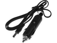
CL power adaptor 12/24V
Cigarette lighter power adaptor for vehicles. 12/14V
Product canceled
-

Cinterion BGS2T terminal
The Cinterion BGS2 Terminal is a simple plug and play M2M device that quickly delivers powerful Quad-Band 2G connectivity and TCP/IP connectivity based on GPRS class 10 data transmission with outstanding low power consumption.
Product canceled
-

Back-Up power supply 12V
Product canceled New product Available
-

5V STE power adapter - USA
5V STE power adapter - USA
Product canceled New product Available
-

5V STE power adapter - EU
5V STE power adapter, EU version.
Product canceled New product Available
-

2x L profile A size
Wall mounting profiles for metal-cased HWg devices Poseidon2 4002 and Poseidon 2250.
Product canceled
-

12V Wall plug adaptor – UK
12V Wall plug adapter - UKUK power adapter 12V DC for devices with 6.3mm barrel jack socket.
Product canceled New product Available
-

12V Wall plug adapter – USA
12V Wall plug adapter – USA
Product canceled New product Available
-

1-Wire hub Power
Power-boosted hub for the 1-Wire bus. Compatible with 1-Wire and 1-Wire UNI bus.
Product canceled
SW application
-
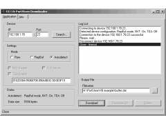
PortStore2 Downloader
Windows and Linux utility for command-line for download the data from PS2 with the autodetection of PortStore2 PL configuration.
Product canceled
-
PD Trigger
PD Trigger
Product canceled New product Available
-

HWg-Trigger
HWg-Trigger is a Windows software utility that alerts to a failed device (out of 10 listed), starts applications, or redirects alarms to text messages (SMS). An action (e.g. displaying a pop-up message) can be assigned to each condition (e.g. a sensor rea
Product canceled
-
")
HWg-SDK (Software Development Kit)
HWg-SDK is a package of programming examples and APIs for various HW group products. Various programming languages, Unix, Windows and other programming platforms.
Product canceled
-

HWg-PDMS
Windows application for collecting data from sensors and inputs over GSM (HWg-Ares) and LAN (Poseidon, Damocles, HWg-STE, HWg-PWR). Export of data in the background. Simple data processing and analysis in MS Excel.
Product canceled